[@DwarkeshPatel] What will computer chips look like in 2045?

Link: https://youtu.be/frYSOKvNiiE
Duration: 69 min
Transcript: Download plain text
Short Summary
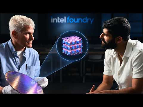
An investigative look inside Intel's fabs and R&D labs, hosted with Chris Auth, who leads development of all Intel processes currently under manufacturing, and featuring Kevin Fischer, Pushkar Ranade, Tyler Osborn, and Jack Kavalieros. Intel's AI-driven demand is running 40-50% above its maximum capacity, and the episode traces why it fell behind TSMC on EUV — the 10nm hyperscaling delay, missing the 2019-2023 EUV window, and a foundry model built around PDKs. The payoff is a look at what's next: 14A with High-NA EUV, backside power, gate-all-around, CFET stacking, ruthenium interconnects, and hybrid bonding.
Key Quotes
- "Easily 40-50% above our maximum capacity, which I’ve never seen before." (00:00:09)
- "What we’ve learned is that you don’t want to do too much innovation in one node, because the more innovation that you do, the more complex it becomes." (00:02:57)
- "Now, at the end of the day, 10 nanometer is a great technology. It has world-class yield, it has world-class performance, it has world-class cost, but it took us longer to do that than what we would have liked." (00:04:27)
- "Well, you don’t want to tackle something before you have to. If you have these other things that can drive performance, you would go and do that." (00:10:18)
- "One thing you learn in this industry is that you will never have a complete data set. If you want to wait for a complete data set, you’ve waited too long. It’s already too late." (00:25:03)
Detailed Summary
Intel Inside: Process Technology, the EUV Gap, and What Comes Next
Episode Framing and the AI Capacity Shock
The episode examines Intel’s semiconductor process roadmap through access to its fabs, process labs, and research facilities, with the discussion centered on how Intel plans to close its manufacturing and technology gap with TSMC. The central concern is that AI-driven demand is already running far beyond the industry’s available leading-edge capacity.
- A two-day tour of Intel’s fabs provided the basis for the reporting and gave the episode direct access to cleanrooms, process-development labs, and Intel’s research arm.
- Chris Auth leads development of every Intel process currently under manufacturing. The other featured specialists are Kevin Fischer on node integration, Pushkar Ranade on equipment and process flow, Tyler Osborn on advanced-packaging technology development, Jack Kavalieros on research, and an Intel advanced-packaging researcher.
- AI-driven semiconductor demand is running approximately 40%–50% above Intel’s maximum capacity, a shock described as the largest the industry has encountered. Leading-edge output is constrained less by the theoretical designs than by the availability of specialized tools, particularly ASML’s EUV lithography systems.
10nm: The Delay That Reset Intel’s Process Strategy
Intel’s 10nm node became the defining example of how concentrating too many innovations in one process can compromise execution. Its main lesson was that a technically strong node is less valuable if it misses customers’ schedules or takes too long to reach reliable manufacturing.
- Intel originally targeted 10nm for 2016, did not begin manufacturing it until 2018, and saw its final products slip by almost four years.
- The node used “hyperscaling” without the new tools that would have supported it, adding substantial complexity for engineers and making schedules harder to control. Despite the delay, Intel ultimately achieved what the episode describes as world-class yield, performance, and cost.
- Intel now limits the amount of innovation attempted in each node and uses a formal “phase gate” system. Yield, defect density, and performance must meet defined maturity criteria before a technology moves from pathfinding into development; designs that miss those criteria are shifted to a later technology.
- The interviews took place against an immediate market contrast: Intel experienced its worst trading day in four months, with its stock down more than 15%, while Taiwan Semiconductor rose 13%.
The Missed EUV Window
Intel’s decision to defer EUV during the definition of 10nm created a compounding disadvantage once TSMC moved first. The resulting gap was measured not merely in years of calendar time but in accumulated experience operating the most advanced lithography systems.
- When Intel defined 10nm, it concluded that EUV was not yet mature enough and reserved the technology for a later node. EUV prints patterns using 13.5-nanometer-wavelength light, approximately 14 times shorter than the wavelengths used by preceding generation tools.
- TSMC entered EUV volume manufacturing in 2019 and expanded its use on the 5nm node in 2020. Intel’s first EUV-based process did not reach products until 2023, giving TSMC roughly four additional years of EUV manufacturing experience.
- For 14A, Intel is adopting High-NA EUV, which retains extreme-ultraviolet light but increases numerical aperture from 0.33 to 0.55. This permits features to be printed approximately 1.7 times smaller in a single exposure.
Transistor Milestones and Intel’s Sequencing Decisions
Intel’s transistor history shows that major concepts often existed long before they could be manufactured reliably at scale. Intel deliberately sequenced its roadmap around technologies that could deliver near-term performance gains rather than moving immediately to the most radical structure.
- The planar MOS transistor was demonstrated in 1960, FinFET was demonstrated in a laboratory in 1989 and entered volume production at Intel in 2011, and gate-all-around was demonstrated in 1988. Samsung did not begin producing gate-all-around chips until 2022, meaning ideas developed around the same period reached production roughly a decade apart.
- Auth says gate-all-around was understood as an idea in the 1990s, but Intel first advanced through strained silicon, high-K metal gate, and FinFETs. Those intermediate technologies supplied performance gains while gate-all-around—which he calls the ultimate transistor—was left for a later generation.
- Taking gate-all-around to high-volume manufacturing required new materials, deposition gases, and tools with specialized characteristics such as a heating chuck. Tool vendors had to invent new capabilities, and engineers had to test multiple transistor structures iteratively, making the path to volume production far longer than the initial laboratory concept.
- Fischer characterizes gate-all-around as somewhat inevitable as the ideal structure given advances in both transistors and interconnects. Backside power, by contrast, was considered much more radical at that time because it required stripping the silicon substrate and rerouting power delivery.
The R&D Golden Age and Rising Process Complexity
Auth describes a broad change in semiconductor research between the predictable scaling era of the 1980s and 1990s and the more experimental period that followed. New materials and process-control methods transformed the scale of what an R&D team could attempt within a single node.
- During the 1980s and 1990s, Dennard scaling and advances in lithography produced a relatively predictable cadence of smaller, faster, and more reliable transistors. By the 2000s, that approach was no longer sufficient, beginning a golden age that included strained silicon, high-K metal gate, FinFETs, gate-all-around, and backside power.
- The number of materials used in semiconductor processes has likely increased tenfold since the 1990s. Atomic layer deposition gives engineers atomic-level control over material deposition, while the R&D mindset shifted from avoiding unnecessary process changes to actively rebuilding processes around new ideas.
- Technology planning retains roughly four years of direct visibility, and engineers can extrapolate another four years from that. Beyond approximately ten years, however, it becomes difficult to predict with confidence what the process or device architecture will look like.
14A, Backside Power, and the High-NA Debate
Intel’s 14A program depends on combining High-NA EUV with backside power, allowing front-side signal wiring to remain less compressed than it would be in a comparable process without backside delivery. Intel and TSMC consequently reach different economic conclusions about the same High-NA tool set.
- When features become smaller than a lithography system can print directly, manufacturers split the pattern across multiple passes; the tightest patterns may require two, three, or four exposures. Each additional pass consumes time on a machine costing around $200 million and creates more opportunities for defects, while a High-NA machine costs roughly twice as much.
- Backside power moves thick power-delivery lines from above the transistors to the back of the wafer. That frees front-side area for signal lines, allowing less aggressive pitch scaling and, in Intel’s case, a single High-NA print where TSMC’s tighter front-side requirements may require double-patterned EUV.
- The economic consequence is that High-NA does not yet make sense for TSMC’s current process approach, while Intel’s backside-power architecture makes it more useful. The disagreement therefore centers on process architecture and tool economics rather than on whether the machines themselves work.
- Intel has worked on 14A for more than three years, is finalizing its manufacturing tool set, and is fine-tuning roughly 2,000 process steps for repeatable operation on thousands of wafers per week. Roughly 80% of the tool set can be reused from 18A, although denser geometry requires new capabilities and some unique tools.
From IDM to Foundry: Why PDK Maturity Matters
Intel’s long history as an integrated device manufacturer did not prepare it for the process-design-kit discipline required by an external foundry. The shortcomings associated with 18A’s initial PDK have changed how Intel tracks process readiness for customers.
- Intel historically operated as an IDM and made only its own chips without using a formal foundry-style PDK. When 18A began without one, public reporting cited delayed instructions and broken guidance for prospective users.
- Intel now tracks PDK maturity against graded targets such as 0.5, 0.9, and 1.0, and 14A is intended to ship with a high-quality PDK from the beginning rather than being retrofitted after the process is defined.
- A PDK describes both the menu of devices a process can build and the rules customers must follow. Intel now allows outside companies to commission chips using its process kits, with High-NA available as a customer-specific option in the 14A PDK.
- TSMC’s foundry scale is presented as an important source of its advantage: serving many customers provides more wafers to learn from, more revenue to reinvest, and stronger deadline pressure. TSMC ships upward of three times as many leading-edge wafers as Intel.
Manufacturing Engineering: Finding and Eliminating Defects
Bringing up a leading-edge node requires Intel to find defects, determine where they originated, and choose among thousands of possible experiments with limited time and wafers. The company’s internal organization is designed to accelerate urgent material through the factory without allowing that urgency to overwhelm overall tool efficiency.
- Intel detects defects through inline metrology tools that inspect wafers and identify suspect locations, as well as through end-of-line electrical testing and sorting. Failed devices are then cross-sectioned to identify the process step responsible.
- “Hot Topics” meetings establish node bring-up priorities, including work on 18A and 18A-P. Fischer and integration engineers use those meetings to direct experiments and align scarce resources across thousands of potential issues, making the reviews a bottleneck for the most advanced node.
- Fischer’s strategy is to investigate multiple potential fixes in parallel rather than assume the obvious diagnosis is correct. Engineers must also decide how much risk to accept when moving to risk production and cannot wait for a complete data set, because the schedule may already have become unattainable.
- The average engineer may have little visibility into how a node’s schedule affects Intel’s financial results and customers, even though decisions about defects and experiments directly determine whether the node can ship on time.
- Intel uses tiered “hot boxes” that give urgent material progressively higher factory priority. HotBox 1 moves through every tool first, but this can reduce overall tool efficiency by disrupting the normal flow, analogous to reserving one highway lane exclusively for a carpool.
- One example is an epi nodule, an abnormal crystal growth that can short one epitaxial structure to the wrong adjacent structure and stop the transistor from working. The discussed responses included a special clean to eliminate the nodule and work to identify its source.
Interconnect: Copper, Cobalt, and the Case for Ruthenium
The shrinking dimensions of chip wiring are forcing Intel to reconsider the metal stack above its transistors. Copper remains effective for many dimensions, but tighter lines expose the growing burden of liners and resistance.
- A modern chip contains more than a dozen layers of copper interconnect above the transistors. At the 10nm node, Intel moved from copper to cobalt, which initially produced stronger results.
- Collaboration with Intel’s external equipment and materials ecosystem later produced solutions that restored copper as a competitive option. Fischer also identifies ruthenium as a possible successor for the tightest future dimensions.
- Ruthenium can be etched into a line and therefore does not need the liner required for copper deposition. Around the 20-nanometer pitch range, its resistivity and conductivity become better than copper’s, while the liner had previously represented a significant portion of the total conduction path.
- Copper is expected to remain the best choice for larger lines, but Fischer believes the tightest copper wires will inevitably need to be replaced. The unresolved question is where the precise crossover occurs and whether ruthenium becomes practical at scale.
CFET: Stacking Transistors in the Laboratory
Intel’s CFET research attempts to place n-type and p-type transistors directly above one another, doubling transistor density in principle while introducing a new class of manufacturing and thermal problems. The laboratory work uses simplified vehicles to separate individual device questions from the full difficulty of a production process.
- CFET stacks complementary transistors rather than placing them side by side, potentially fitting twice as many transistors in the same area. Every added layer also adds process steps, cost, and heat, and the episode describes no clear escape from those penalties.
- Vertical connections replace routing that previously ran above or below the transistors, making trench aspect ratio, trench filling, and the risk of unfilled air gaps increasingly difficult. Intel, competitors, and external laboratories are all evaluating the architecture.
- Intel has fabricated a simplified CFET-style stacked nanoribbon transistor with one wire for the NMOS and one for the PMOS rather than four ribbons on four. The reduced structure lowers the aspect-ratio challenge, while the laboratory features are already at least as small as production features.
- The research also includes atomic-monolayer two-dimensional materials, including transition-layer dichalcogenides, and structures printed using EUV or electron-beam technology. These examples show that CFET evaluation is not restricted to conventional silicon nanoribbons.
- Intel uses short-loop test vehicles for faster iteration because a normal manufacturing flow can take a month or longer to complete thousands of steps. The loop first qualifies unit cells such as diodes and capacitors before combining them into more complex vehicles such as the transistor itself.
- Novel materials and complex architectures fail for different reasons. New materials must support deposition, etching, removal, and compatibility with surrounding layers, while CFET’s apparent simplicity still requires roughly a thousand process steps to work together.
- Of roughly 20 candidate material ideas such as two-dimensional materials, some fail because no contact adheres despite successful deposition and measurement. Others are destabilized by gas interactions in later steps and require hermetic sealing; if that sealing cannot be controlled, the idea is treated as a dead end.
Monolithic 3D Logic and the Future of Memory
Gate-all-around transistors and backside power are changing the physical relationship between logic devices and their wiring. This shift opens the possibility of monolithic 3D logic, although thermal limits complicate combining dense memory stacks with processors.
- With transistors effectively floating within the interconnect structure, monolithic 3D stacking becomes conceivable rather than merely speculative. NAND already uses this form of vertical integration, while DRAM is expected eventually to move in the same direction on a 10–20-year timeline.
- Logic consumes more power than memory, making it difficult to integrate logic directly with dense stacks such as HBM or 3D NAND. Heat is the central obstacle to such combinations.
- Three longstanding constraints limit compute performance: switching frequency, power efficiency, and thermals. These are not new problems, but system-level analysis and simulation tools for fully integrated 3D devices remain in their infancy.
Inter-Chip Interconnect and the Area-versus-Perimeter Problem
Advanced packaging addresses a different constraint from transistor scaling: how separate chips move data to and from one another. In AI systems, that traffic can limit workload completion even when raw computation capability is available.
- In Nvidia’s Blackwell data-center GPU, two large processor dies are surrounded by eight stacks of high-bandwidth memory, creating a system in which the chips must exchange data continuously.
- The “area-versus-perimeter” problem arises because doubling a chip’s width and length produces four times as much area for circuitry but only twice as much edge length for connections. Computation therefore grows faster than the available bandwidth for moving data across the chip.
- Packaging evolved from side-by-side chips connected from their edges, to a shared silicon interposer supporting a “2.5D” arrangement, and then toward hybrid bonding.
- Hybrid bonding aligns copper interconnects on two chips, brings the surfaces together, and heats them so the copper expands and bridges the gap. This replaces bulky, resistive solder bumps with much denser connections and is only now entering volume manufacturing after years spent resolving alignment and defect issues.
Deterministic Computing and the Jane Street Debugging Tool
Intel’s Processor Trace illustrates how much production software depends on execution behavior that conventional test tools cannot easily reproduce. The episode presents both an internal debugging success and an external effort to eliminate nondeterminism at the hardware boundary.
- Intel’s Processor Trace has existed for roughly a decade and, when enabled, records the code a program executes in enough detail to reconstruct individual function calls.
- Jane Street needed to investigate fleeting events such as delayed responses to network packets that most debugging tools could not capture. An engineer discovered Processor Trace and, together with a summer intern, built “magic-trace,” which presents the function-call history leading to a selected moment of interest.
- The magic-trace project began as a bottom-up effort by one engineer who believed it would be useful. Traders and developers throughout Jane Street now use the tool every day.
- Osborn explains that Intel has spent more than 50 years optimizing CPUs for speed, but caching, branch prediction, and speculative execution reduce predictability. The same instruction sequence can take four cycles on one execution and 300 on another, creating difficult-to-reproduce behavior across threads and cores.
- Antithesis built a 100% deterministic computer by identifying every route through Intel’s x86 architecture through which nondeterminism could enter, including network packets, disk reads, temperature sensors, and time itself. It then either closed those routes or substituted controlled simulations.
- On that foundation, Antithesis created a testing platform that compresses years of production hardening into minutes. It runs software through thousands of parallel worlds, injects faults, steers them toward a one-in-a-billion failure, and can reproduce the resulting bug and trace it to its root cause.
Wafer-to-Wafer and Chip-to-Wafer Bonding
Intel expects both wafer-level and known-good-die bonding approaches to remain relevant, with the choice determined by the customer and architecture. Hybrid bonding is also pushing interconnect pitch below the dimensions used in today’s highest-volume packaging.
- Wafer-to-wafer bonding, described in the discussion using Intel’s die-to-die terminology, already dominates the CMOS image-sensor market and is being examined for memory stacking. It requires mirrored, left- and right-handed die arrays that match perfectly; when sort-good arrays do match, all good dies can be bonded, but the odds of such an exact match are low.
- Chip-to-wafer bonding allows dies to be singulated and tested individually so that known-good dies are bonded to known-good counterparts. Both approaches will be used, and chip-to-wafer is particularly suitable for logic-to-logic applications.
- First-level interconnect pitch has fallen from approximately 130–150 micrometers about 15 years ago to 25 micrometers in Intel’s Foveros production technology. Sub-10-micron work is already underway.
- A paper presented at the May IEEE ECTC conference, described as the industry’s largest annual packaging conference, reported reliability data for a hybrid-bonded device with 0.45-micron pitch. That represents approximately another order of magnitude in density beyond current high-volume manufacturing.
- Typical back-end fabrication layers below packaging are around 1 micron to half a micron, so packaging at 0.5 micron or below could connect lower silicon layers and reduce total IR drop. For client devices, hybrid bonding’s principal benefits are raw interconnect density—especially between a CPU and GPU—and lower total interface power measured in picojoules per bit.
The Equipment Supply Chain and Manufacturing Economics
Leading-edge capacity is constrained by specialized tools whose supply cannot expand as quickly as AI compute demand. Intel’s own execution problems therefore exist inside a broader industry-wide shortage of lithography, process equipment, and advanced manufacturing capacity.
- ASML produces fewer than 100 EUV tools per year and does not plan to produce significantly more than 100 annually, even by the end of the decade. That capacity must be divided among Intel, TSMC, and memory manufacturers such as SK Hynix that are ramping production.
- Ranade says Intel is a bottleneck but not the only one, because all equipment is in severe shortage. Process lock-in makes substitution difficult: once 18A is built around a specific tool, another tool from a different supplier generally cannot simply replace it.
- The available tools are nowhere near sufficient to produce ten times the current leading-edge wafer output; approximately a twofold increase may be possible. Over the same decade, the AI industry has roughly tripled compute year over year, so continued scaling requires the entire equipment supply chain to expand.
- A couple of billion dollars of Intel capital expenditure, amortized over many years, can produce enough logic for roughly $100 billion in annual revenue for AI model companies, before adding the value of memory and other stack participants.
- Once a fab is built, approximately 80% of its cost structure is fixed. Additional utilization and yield therefore produce disproportionately large revenue gains, and increasing die yield from 60% to 65% or 70% is not a linear improvement.
- Only three foundries remain at the advanced node, compared with roughly 20 forty years ago. The consolidation reflects the scale economies required to operate leading-edge fabs.
- The industry moved from a largely vertically integrated structure 30–40 years ago to a horizontal ecosystem of foundries, equipment makers, and component suppliers. It is now shifting toward a “pseudo-vertical” model because hyperscalers design their own chips and model-company demand can consume an entire fab’s output or more, funded by the customers themselves.
Intel Versus TSMC: Scale Rather Than Technology
Ranade argues that Intel’s remaining competitive gap with TSMC is primarily about manufacturing scale and execution rather than a major technology deficit. The relevant measures are timely production, high yield, and the ability to support rapid customer ramps.
- Intel is at most a few percent behind TSMC in performance, power, or area density, according to Ranade. He considers differences of that size less important than whether a node ships on schedule and can ramp large volumes at high yield.
- Ranade disputes SemiAnalysis’s claim that 14A, due in 2028, would be comparable to TSMC’s N2 in transistor density. He notes that a node is a bundle rather than a single metric, including low-leakage and high-drive-current transistors, high-density and high-performance SRAM, analog, and RF.
- Under his framework, foundry comparisons become meaningful mainly when one process is a full generation or two behind. If the nodes are otherwise close, density comparisons can amount to “splitting hairs” while missing larger differences in execution and scale.
The Current Roadmap and Production Discipline
Intel is attempting to convert the lessons of 10nm into a more disciplined operating model for 18A, 18A-P, and 14A. The near-term objective is not simply novel device designs, but processes that can be manufactured repeatedly, supported by mature customer kits, and ramped at scale.
- Intel is currently ramping 18A, has 18A-P in development, and is fine-tuning 14A while finalizing the tool set required for production.
- Each node now carries less innovation than 10nm attempted, with phase-gate criteria determining whether a design is ready to advance. PDK maturity is tracked alongside process maturity so outside customers can adopt the process without repeating the early guidance failures associated with 18A.
- The overall approach combines High-NA EUV, backside power, gate-all-around transistors, a more deliberate interconnect-material strategy, and advanced packaging. Its success depends on translating those technologies into timely, repeatable, high-yield manufacturing rather than treating them only as isolated laboratory advances.